
Electronic Design and Family Site
Experiments in DDS
- In this exercise, I wish to develop a series of DDS VFO modules that can be adapted to a variety of uses:
-VFO for a traditional Superhet rig
-I/Q VFO for a Phasing-type rig
-Signal Source for Test Equipment
-Wideband VFO for Direct-Conversion rigs
These modules will all have a few things in common:
-Self contained: plug-in units that can be easily inserted into any project
-Consistent hardware platform: to aid both software adaptation and make Plug-In compatibility easier.
-Easily Configurable software: so I don't have to play with it much to adapt to the parent application
30 May 12
-I have built a PCB that contains just a AD9854 DDS, clock, 3.3V regulator, and output filters. It is based on AA0ZZ's IQ-Pro RF board. I always had issue with putting two different voltage rails on the same PCB (I've blown the parts on his board several times!!), so I will not include the amplifiers on this PCB; they will be separate allowing me to optimize them once the rest of the device is operating properly. This PCB has a header to receive the Digital Control Signals so I can run it from essentially any microcontroller.
Once built, I plan to test its proper operation using either the I/Q VFO, or I/Q-Pro kits that I own. Once proper operation is confirmed, I will begin by modifying the code of the I/Q-VFO kit to meet my needs; it uses cheaper, more readily available PICs. Hopefully, I can get all of the code into a single PIC like the PIC-EL kit does. If that's possible, I hope to migrate into a 18F2520. It has enough I/O to accomplish anything I would want.
7 Jun 12
-I've decided that it's just too much work to slowly move this project through several iterations of PIC-type and software just to arrive at using a 18F2520. Each new device or PCB requires at least a re-write of the ports, and in some cases, a complete re-write of the firmware. Thus, I've designed what could be the final PCB using a 18F2520, an standard HD44780 LCD, 4 pushbuttons, and a Rotary Encoder. Once the PCB is assembled, I will begin writing the code.
17 Jun 12
-Father's Day interrupted the flow of work slightly, but I got a chance to etch and start drilling the digital board. It's about 2-1/2" by 2-1/4". More to follow...
21 Jun 12
-I have placed the AD9854 schematics on the website. I've also included the Digital PCB Layout X-Ray views.
2 Jul 12
- Field Day and some personal time took me away from my DDS endeavors for a couple of weeks, but I'm back for the time being. I finished populating the RF board last night only to discover the 3.3V line was shorted to ground. I have a high-powered stereo microscope available at my work place, so I have to wait until I can go there to inspect it.
Since winter is usually better for me to write code, I plan to get all of the hardware built during the summer and start on the code when the weather turns bad in the fall. Thus, when I have the 9854 hardware working well, I will start on 9851 hardware.
3 Jul 12
- I inspected the PCB thoroughly and found nothing wrong. Then I started removing components. It was a capacitor. Once I removed one, the short changed to about 500 ohms. Simple enough! Now work can progress.
14 Jul 12
- Last weekend I traveled out of town for business; no progress whatsoever on the DDS. This weekend, I've been working on a AD9850-based VFO. I plan for this to be a single board the same size as the LCD. It will plug into the LCD and the LCD mount will support both boards. This companion board contains the PIC (18F2520), the DDS (AD9850 or 9851), the clock oscillator (100MHz to 125MHz), and some filtration of the DDS output. It will have a header for the Rotary Encoder and pushbutton inputs.
23 Jul 12
- The 9850 board is as complete as I can currently make it. I don't have the 100MHz clock oscillator (actually, I have 2ea 125MHz, but they're 3.3V, not the 5V I need for this circuit!), so I'll have to order and wait. I want to mount the 9850 last, so that also isn't mounted. Some of the bypass capacitors have to mount after the 9850.
I tried to save the final PCB patterns out to place on this page, but realized I'd put the cart before the horse; I laid out the PCB without a schematic. Thus, I must first draw a schematic of the circuit, complete with reference designators, then I can label the PCB and put it on this page. Look for that in the upcoming days.
I expected I wouldn't get to the programming of these projects until the colder weather starts, but by a stroke of luck, I've been given a week to play with it. I have to attend some training out of town soon. Sitting in a hotel room after the training day ends, there's very little else to do but write code. Thus, in a few weeks these projects will advance. In the meantime, keep an eye on the "Other Projects" page as I try to write up some of the woodworking and "other" projects I do.
25 Jul 12
- I have completed the schematic and thus, the PCBs. They are all posted to the appropriate pages linked above. I have ordered the 100MHz 5V oscillators for the AD9850-based VFO as well. They should arrive by early next week. In the meantime, I've been working on the PCB layout for my version of a NorCal Sierra in which I hope to use the 9850-based VFO. Using a DDS would save a ton of circuitry in the rig: PMO Filters and mixers, RIT circuitry. Obviously though, before I can build the rig, I have to get the VFOs going, so code will be next up on the agenda.
2 Aug 12
- I made a stupid error on the original 9850 design: I wasn't watching Port assignments very carefully when I assigned ports and pins to the various functions. Thus, I assigned the LCD data pins on the PIC reversed from the order of the LCD. I could have written a subroutine to swap the bits and reassemble them correctly, but it seemed better to make the PCB correct at the front of this process; it will make code generation simpler in the future. So I have another PCB to make, and some parts to uninstall.
I have started on the code. I am basing this project on the PEGEN 6 code designed for the PIC-EL trainer, written by Craig Johnson, AA0ZZ. Other than modifying for the 18F2520, and changing the port assignments, the only large modifications I must make are to have it read band information from the plug-in modules rather than from operator input, and add (or actually subtract) the IF offset. Otherwise, I'm perfectly fine with how the original design intent is implemented.
10 Aug 12
- The new PCB is complete and populated. It's physically much improved...the LCD fits better, making a much more compact unit. With the LCD position changed, I can also better access the PIC for reprogramming.
As I mentioned previously, this project probably won't be completed until the fall or winter. I want to continue making hardware while the weather is nice. When the weather turns colder, I plan to move my fun indoors and focus more on the programming side of things. This allows for another efficiency: when working in code, I get into "Code-think" mode. In that mode, my thought processes are slightly different and ideally suited to writing code. After a few weeks of not programming, I forget all about thinking in binary or which ports carry which peripherals. Thus, it's better to line up the projects and stay in programming mode as long as possible.
Thus, the next project coming up is a redesign on my SWR/Power meter. I plan to split them up into separate meters in much smaller chassis. I also hope to eventually write a book on homebrewing based on the LCD RF Power Meter.
14 Oct 12
- The weather has turned cold and rainy: perfect time to write code. I'm starting on a 9851-based VFO tentatively planned to go into a NorCal Sierra-based Xcvr. As with all of my PIC programming, writing functional code is like pulling teeth: I write something that sounds utterly reasonable, it fails for side issues like banking or dual-instruction program counters; I settle those issues, then have to deal with one or two typos that keep the program from functioning at all and are "untroubleshootable".
In this particular case, I spent two days playing with a binary-to-BCD converter and never getting it working. I think it's an issue with indirect addressing. Regardless, I discovered a simpler and more elegant way of implementing this function and it (finally, after clearing some typos!!) works well. Next up: I plan to enable a Band-switch read to a table from which to draw band information.
23 Oct 12
-The table read started out working rather oddly until I remembered that the start of each discrete frequency is 4 lines down from the last. Thus, I multiplied my table-read value by 4 and it worked well and displayed properly on the LCD. But, the DDS isn't singing. I found that the register names for indirect addressing between the 16F- and 18F-series PICs are different, so I need to change the names. I also discovered that I had the DDS ports set incorrectly. The DDS is on Port A, but I had the output sigs going to Port B. It's always the stupid typographical errors that keep me running!!
1 Nov 12
-I don't have any idea why, but I simply can't get the DDS to operate. I can see what appears to be the proper signals on the proper pins; when I compare to the PIC-EL, it seems to be doing precisely the same thing. I've swapped the DDS in the hope that I had a bad one, but no dice. I verified the layout when I had the chip off, but it looked fine in comparison to the schematic. Since I have created both the PCB and software, I can't know which is at fault.
...so I have a couple of cheapie AD9850 modules on order from E-Bay. I assume that I can count on them to operate (however briefly), and I can use that to verify my code. The worst downside is that I have to wait 2 weeks for them to ship from China. More to follow...
1 Dec 12
-After a well-deserved vacation and upon the arrival of the cheapie modules, I've resumed work on this project:
I plugged a module into my PIC-EL to verify that they're functional. It worked. I'm a bit surprised actually, because the two lower bits of the parallel data word were not tied high: a state that is supposed to be necessary for serial programming. Regardless, it worked. I then plugged it into my circuit: No luck. I then plugged a DDS-30 into my circuit...no response. Thus I've proven the issue is with my circuit (or code). The next step?
I will ensure any "side" issues are covered such as adding capacitors to the power rails on my circuit and using an actual power supply rather than a 9V battery. I've watched the clock, data, and update pulses going to the DDS chip; I know they're there. If I must, I'll wire three DPST switches to the data inputs and manually program the DDS to understand what they need (vs. what I'm providing).
This is a quest!
28 Dec 12
-The problem I left off with was as trivial as I expected: I had set the Port for the DDS outputs as a digital output, but never told the PIC not to make it an ADC input. Thus, while I was providing digital outputs on that port, I was also dragging those outputs down feeding the device's internal ADCs. Once I turned the ADCs off, voila!
Once that was done, I tried to get the Encoder to work. No dice. I have no idea what wasn't working, but after 3 weeks of screwing with it, I essentially abandoned the code I was using as a model and struck out on my own.
I stuck with the routines I knew worked: The LCD routines, the band read and lookup table, the DDS computations, the mechanism to send words to the DDS, and all of the initialization. I then started writing code. So far, the encoder is working, but marginally: it knows direction about 30% of the time. It counts in random "steps", and occasionally gets stuck in a count and keeps stepping up or down until I rotate far enough to stop it. It isn't perfect, but it's progress.
5 Jan 12
-Success! When I left off, I had issues with the encoder. It was a minor syntax issue; in a series of commands, I was copying the address of a variable rather than the data it contained. That caused the random steps and getting stuck in wierd loops, because it was accessing random program addresses rather than simply manipulating data. A simple change from MOVFF to MOVLW cleared that up.
Then, I added a routine to to either add or subtract an IF value, and added a table to tell which bands added, and which subtracted. That was relatively easy to implement.
Finally, I've spent the past week...about 12 hours total, simply getting the unit to read an input and process the IF or not. This is for a CW transceiver; it uses an IF in receive, but will transmit directly on frequency. My first approach didn't work at all. I then looked at how AA0ZZ did it in his I/Q-Pro VFO. I copied his subroutine to watch the port, set several variables, and change the display. With that added, when in transmit, the DDS frequency wouldn't move. I realized that the subroutine to process the IF was the only place that updated the frequency information for the DDS. Thus, I also had to add a subroutine to copy the freq information directly into the temp registers the DDS used. With that accomplished, I thought I was done, but then I couldn't get the program to change between processing the IF, or bypassing the processing. Whichever command appeared first after the BTFSS or BTFSC processed. I went as far as adding a switch followed by two display commands so I could determine whether the appropriate bit was being set. My best guess is that I exceeded the nested subroutine limit of my device. After literally 8 hours of efforts, I found a way to bury the "bypass" routine within the IF Processing routine, and voila...it finally works.
Once I clean up the code and make it presentable, I will post it here. Since switching IF processing in and out is unnecessary for one, I long-ago inadvertently had a version of code that should work with a SSB rig. Thus, once I get that code cleaned up, I will also release it.
Next up...VFO for a BCB AM receiver. When that's done, I will tackle the AD9854 phased xcvr code.
31 Jan 12
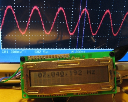
-I now have the 9854 code working. All of these codes are quite simple; they read an initial band and load that frequency into the DDS and LCD. Then they scan the rotary encoder looking for a change. If a change is detected, they determine direction and either add or subtract a "step" value based on which digit is being varied. A pushbutton switch further selects the digit to update (ones, tens, hundreds, thousands, etc.). To the 9854 code, I recently added a sideband-select function so I can switch a relay for sideband selection. I may stop there and move on to other programming while the weather is still tough!
18 Feb 13
-I've spent the past couple of weeks making PCBs for separate SWR and RF Power meters. As long as I'm set up for programming and in the "programming mode", I want to continue writing all of the PIC code I could forseeably need. In the case of the DDS programming, all I needed for hardware was a board to hold the clock, PIC, DDS, LCD, and regulator. In the case of these meters however, I need to make the entire hardware before I can even begin programming. Thus the delay.
28 Feb 13
- I took the code from an earlier combined SWR meter & Power Meter project and essentially split it by function: I made two boards with the same pinout in terms of LCD ports and analog inputs. Then I used the same "overhead" on the code for both programs and removed the unused code from each (I removed the power and barcoding from the SWR meter, and removed the SWR calculations from the power meter). This left me two very basic meters. Once I figured out config settings and fixed some minor hardware issues, I had two meters that could at least display on their LCDs (I'm working in the house, rather than my shed, so I don't have a transmitter to test the RF functions yet). Now the fun begins as I add more functionality to both meters!
2 Mar 13
- I still haven't mastered PIC Config words. I spent around 3 hours yesterday trying to figure out why the SWR meter came up relatively OK, but the power meter refused to run in any form. I swapped the PICs between the two circuits, and the SWR PIC came up fine in the Power circuit. Thus I knew the hardware as OK. Then, I copied the Config words from the SWR program into the Power program, but it still wouldn't work. Finally, in an experiment, I decided to let MPLab program the Config words, and the power program came up fine. Upon closer inspection of the SWR program, I discovered that I'd let MPLab program its config as well; that's why the SWR program operated despite having the same embedded config as the power...it wasn't using the embedded config!!
I just copied the words from MPLab's setup into my embedded config, but I still want to learn why my code didn't work. Regardless, I now have relatively functional SWR and Power Meters. The next "improvement" is to add battery monitoring. I have many open ADCs, so this should be very easy to do.
11 Mar 13
-I added a battery monitoring function to the Power and SWR meters. I placed a 3:1 divider on the actual battery input past the power switch and input that DC to an unused ADC on the chip. This has turned out to be a royal pain to implement:
What I wanted was to change the last 3 digits of the top line of the LCD with either 3 blanks or the word "Bat", depending on the battery reading. Due to the ADC result testing, I needed to make the digit writing method into 2 separate subroutines. Instead of the typical "Call/Return" that subroutines use, I made a mistake and used "Goto/Return". That ended up sending the program into random places by returning to the wrong place after each of these calls. I discovered this after spending many hours of troubleshooting.
With the code issued settled, I tested the functionality by placing a potentiometer across the +V and ground with the wiper feeding the ADC inputs. On the Power meter, it was OK, but the SWR meter refused to work. Many hours of troubleshooting later revealed that I mis-counted and put the battery DC on a digital-only pin of the PIC. That's why it never functioned. Some quick soldering fixed that, but I haven't yet tested its functionality
Once I was done testing the power meter with Pots in place of the Log amp's output and the Battery DC, I removed the pots and put the circuit to its original configuration. When I powered it up, it displayed the headers, but when it was supposed to start reading, the display blanked. I checked the various analog inputs to discover that essentially all of the ADC and reference inputs were pegged at nearly Vcc. I assume the issue is that I used high-performance wideband Op Amps instead of single-supply DC op amps. Thus, I have a hardware issue to address before I can verify that the software is fully functional. It never ends!
24 Mar 13
The issue last time was in fact that I used the wrong type of Op Amps. I now have simple LM358s installed and both meters are working well. I tried increasing the RF Power meter to 4 digits and using all 10 bits of the ADC, but even with my sample-averaging scheme, the readout was a blur; it constantly "dithered" between several steps of the ADC. Thus, the code for that meter is largely unchanged from that of the original project.
I am essentially shutting both meters down right now and calling them done- a success. Later, I will work on putting them in chassis, but since spring still hasn't arrived, I'm continuing with code-oriented work. I am revisiting the AD9850-based VFOs in that I'm incorporating the 9850 assemblies I bought to verify my hardware setup. Since I have 4 AD9850s mounted with 125MHz crystal oscillators and filters, I want to use them in my various 9850-based projects. They needed a different PCB without a built-in AD9850. Thus, a PCB redesign. I have one about 3/4 built and it looks promising. Once I have one complete, it should be a simple matter of changing the master oscillator multiplier from 100MHz to 125MHz and verifying proper operation. Then I will build the rest of them.
Remember, when working with PICs, whenever I say "should be a simple matter of..." it usually takes weeks and makes me pull my hair out. Let's see where this one goes!!
5 Apr 13
-This project is closed. I laid out, etched, populated, and tested a PCB layout to use the external DDS modules instead of my DDS board. They work every bit as well as my original. I have updated the page so that both my original design, and the PCB to use the modules are both available.