
Electronic Design and Family Site
A digitally switched Filter Bank
A common problem whenever I try to make a rig with more than 1 band is filter switching. Rotary switches won't typically switch more than 2 poles at 6 throws...limiting the number of bands to 6. Even getting such a switch nowadays is tough; they're nowhere near as common as they used to be. Plus, the 2 poles allow access to the input and output of the filter, but offer no means of telling the rest of the rig which band you've selected; more than just "nice to have".
Instead, I decided to make a switch "Bank" that I could insert into any digitally-controlled project. This bank should be relatively small, be PIN diode switched, contain it's own power regulator(s), and for this piece of the puzzle, and for this exercise, be receive-only bandpass filters. By virtue of digital control, the filter bank isn't providing band information to the associated rig, it's receiving the info from the rig.
Below is the result so far...
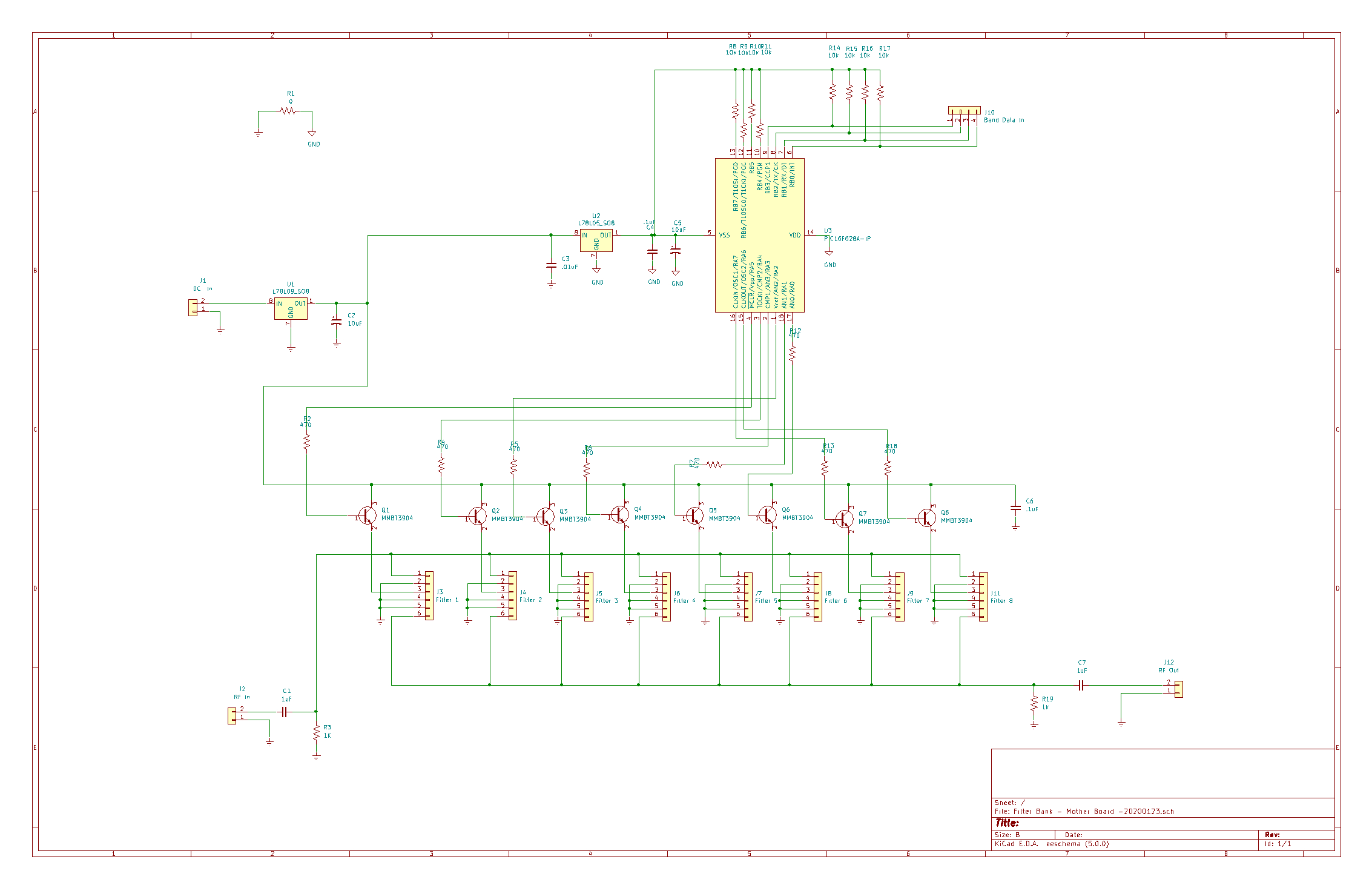
The motherboard regulates power, contains all of the modules input and outputs, contains the switching logic conversion, and has a series of plug-in filters that perform the actual filtration. The logic is controlled by a PIC; I'm sure I could have used a simple BCD to decimal conversion IC, but I wanted the flexibility to determine my own data format, and my own "1 of" output pins. Plus, nowadays PICs are nearly as cheap as logic ICs.
As the schematic above shows, DC input is regulated down to +9V for use in the actual switching. That +9V is then regulated down to +5V for the PIC and filter-select lines.
Whenever data is seen on the data input, the PIC converts that data to raise one of the filter-select lines high. That high enables the associated transistor which sends +9V regulated to the module to drive the PIN diodes.
RF enters the board at either J2 or J12 (the actual filtration is symmetrical, so RF-In and -Out can be swapped), and is filtered by whichever filter module is selected. The filtered RF then leaves by the other RF connector.
Theory of PIN Diode switching is fairly straightforward: When forward biased, a PIN diode will pass RF with very little attenuation; even RF that's greater in voltage than the biasing voltage. Similarly, when reverse biased, a PIN diode will block RF that greatly exceeds the reverse-bias voltage. This is the difference between PIN diodes and normal rectifiers (except 1N4007 as described below). I already had, and used MPN3700 diodes. Their frequency range is a bit above the lower bands, so I made provisions for also using 1N4007 diodes. I know little of their characteristics, but hear anecdotally that they make wonderful cheap PIN diodes. I must be true, even the venerable Elecraft K2 uses them!
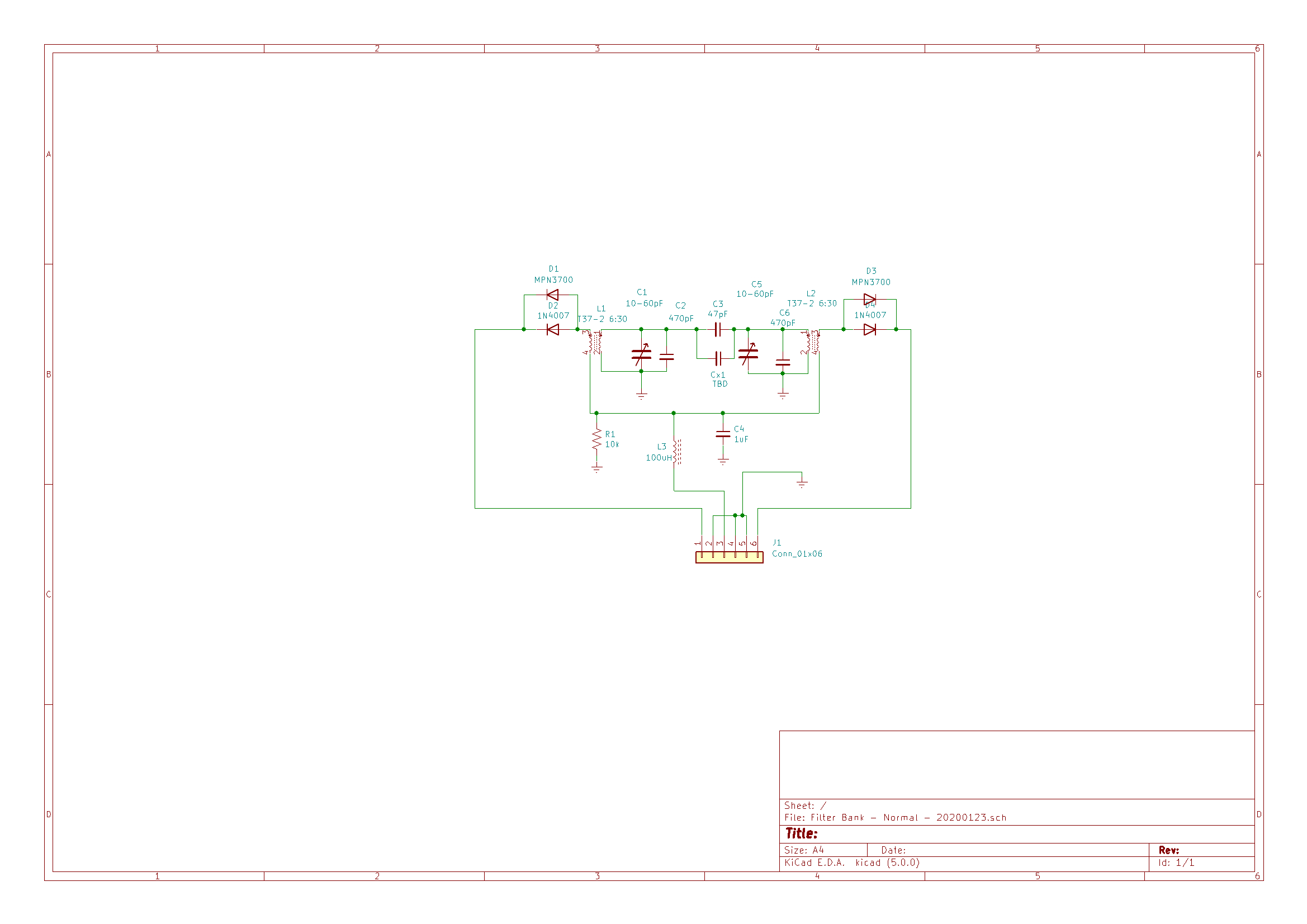
The filter modules are very standard and, I hope, very easy to understand:
The module is selected by about +9V on pin 3. The DC runs through L3 to the diodes at either end of the module. 2 diodes are shown at either end, but only 1 should be installed; whichever is more suitable to the frequency being filtered. Having positive DC at the Anode ends of the diodes makes them conduct. The positive DC that is felt at the cathodes of all other installed modules helps hold them off while this module is selected. R1 keeps the Anodes of the module at ground while the module is not selected (and while the diodes are reversed biased).
Otherwise, this is a very standard double-tuned top-coupled bandpass filter design that many others have used. The values for these filters came from QRP Labs bandpass filter kit.
I have also designed a Low-pass filter module. All concepts are the same.
PIC Programming
The PIC Programming is in progress. Watch this page for the *.asm file.