
Electronic Design and Family Site
GoLiaTH
Circuit Description
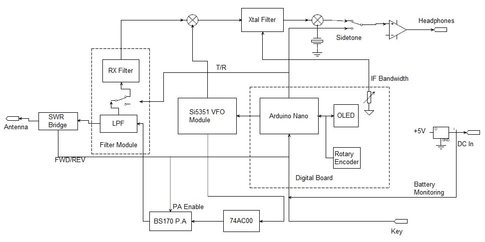

High-Level Circuit Description
Digital Control
All switching, display, and VFO control functions are located on the Digital board. The Arduino Nano initially sets up all operating functions (Switching T/R to receive, un-muting receive, turning PA enable OFF, setting the last used operating band and frequency, and enabling receive audio), then continually looks for changes in any of the switches. If it detects such a change, the function of that switch is started (VFO tuning always has priority): Key-Down switches T/R to "T", Mutes receiver and begins sidetone, disconnects the input of the receiver from the RF path. Pressing the SWR button does the same as transmit except it also receives the FWD and REV power from the SWR bridge, computes SWR, and displays it on the OLED. Pressing Radix changes the digit that is updated when rotating the TUNE control (10K, 1k, 100, or 10 Hz). Finally, rotating TUNE either increments or decrements the frequency by the quantity of the digit selected by the RADIX control setting.
The grounds of all digital circuitry are tied to the analog ground at only place: Pin 8 of J13 on the analog board. All digital circuitry is fed +5V by the regulator on the Arduino, while all analog circuitry is fed by the AZ1117 LDO regulator on the Analog Board.
Receiver
The receiver follows a traditional superheterodyne format. The input signal is first sent through that band's Low-Pass Filter (LPF), then passed through the Receive mute switch to the Band-Pass Filter (BPF) where it is filtered to allow only the band of interest. It is then mixed down to an Intermediate Frequency (IF) in the first mixer which is fed by the VFO and amplifies the signal slightly. This IF is then sent to a variable-bandwidth crystal filter where it is filtered very tightly (bandwidth depends on the setting of the bandwidth control). It is mixed once more to its final audio frequency in the Product Detector which mixes the IF and a crystal-controlled BFO signal. The resultant audio is amplified for speaker-level, switched for mute and sidetone, and fed to a speaker through some RF filtration components..
Transmitter
The transmit is simply amplification and filtration of a single frequency. The transmit signal is generated in the Si5351 Variable Frequency Oscillator (VFO) module at the direction of the Arduino Nano on the Digital Board. That signal is a 3vp-p square wave that is insufficient to drive the BS170 Power Amplifiers to full power. It is first sent to the a single 74AC02 gate to increase its level to 5Vp-p and then to 3 stages of 74AC02 to boost the output current to sufficiently to drive the BS170s. The 3 BS170s operate as class E amplifiers boosting the signal current up to the final drive level.
Detailed Circuit Description
Digital Board...
The VFO signal is computed on the digital board in the Arduino Nano, A1. Initially, the VFO is set to receive at the last saved frequency of the selected band. The band information is sent to the digital board via pin 2, J15. The information is actually an analog voltage sent to A1, Pin 21 as determined by the reult of voltage division deterined by a 1K ohm resistor on the analog board, and the band resistor on each band module. That band-specific frequency is stored in memory and recalled when the Nano powers up. Then, whenever the Rotary Encoder rotates, the pulses are tracked and the VFO digit, as selected by the setting of the Radix switch SW2, is incremented or decremented. This frequency info is then sent out the DATA line, A1 Pin 23 (SDA), to the OLED pin 4, the Si5351 VFO via pin 6 of J15, and stored in memory after 1/2 second of stability. The receive VFO frequency word sent to the Si5351 is the actual frequency minus the BFO frequency, the frequency sent to the OLED is the actual frequency.
The IF bandwidth is determined by the DC voltage presented to the 1SV149 Varicap diodes on the analog board. The entire variable DC voltage circuit is located on the digital board at RV1, R4, C36, and pins 1, 6, and 9 of J14. RV1 varies the +5V at "H", and the 3.5V at "L" (determined by the voltage division of RV1 and R4). This variable voltage is fed back to the Analog board from pin "W" of RV1 via pin 6 of J14. The entire IF Bandwidth variable circuit is isolated from the rest of the digital board to keep digital noise out of the very sensitive IF chain. The analog ground that comes up from the analog to the digital board for this circuit is also used to filter the raw incoming DC used for battery monitoring.
Incoming Raw Battery Voltage is sent to the digital board for monitoring and to feed the digital +5VD regulator, via pin 7 of J15. This voltage is divided between R36 and R37 to reduce the incoming voltage by 2/3 to safely feed the voltage to A1, pin 25. This voltage is then multiplied by 3 to compensate for the resistive divider, and has .35V added to compensate for the loss of the reverse-voltage-prevention diode, in the Nano before being sent to the OLED.
SWR signals, SWR_FWD and SWR_REV are filtered by L2 & C8 and L1 & C2 respectively, prior to being fed to pins 22 and 26 of the Nano. These lines are only actively read when the SWR switch SW4, is being pressed. When that switch is pressed the entire rig is put into transmit (T/R switches to "T", Rx_ENABLE "MUTE"s the receiver, Rx_Mute "MUTE"s the recive audio, and SIDETONE is sent), and the SWR_FWD and SWR_REV signals plugged into the formula: (FWD+REV)/(FWD-REV). The resultant integer is then fed to the OLED for display. When SW4 is released, the rig is placed back into receive, and the OLED display is returned to normal.
Sidetone, when requested by either "Key" or SW4 lines going to ground, is simply a tone generated by A1, sent through a 6-Pole R/C LPF (R15, R16, R17 and C65, C66, C67), to the audio chain through Pin 7, J14. Currently, that frequency is hard-coded in the firmware, but there are plans to make it user-adjustable. The audio switch on the analog board selects either Rx audio or sidetone effectively muting Rx audio when switched to sidetone.
The remainder of the components on the Digital Board are either pullup resistors for the various switching inputs:
R1 - Keying
R3 - Radix
R2 - SWR
...or filtration components to keep RF out of the digital board's circuitry:
C89, L24, C90 - OLED
C36 - IF Bandwidth
C86 - Battery Voltage
C6 - SWR
C7 - Radix
C1 - Key
C10, C92 - Raw Input Voltage
C11, C3 - +5VDigital
C5, C9, C2, C8, L2, L1 - SWR FWD/REV
As mentioned earlier, the GoLiaTH transceiver uses 2 separate regulated +5V supplies to keep RF out of the digital power and keep digital noise out of the analog power. The AZ1117 regulator is for the analog circuitry, and the Arduino Nano's internal regulator is used for the digital circuitry. Similarly, the radio separates its grounds between the 2 circuits for the same purpose. The two grounds meet at only a single point near J13 Pin 8 on the analog board.
Band Modules...
The band modules serve 4 functions:
-Band Switching
-TX and RX LPF
-Tx and Rx BPF
-Band information to the rig
Band switching is accomplished by inserting the proper band module into the corresponding socket on the analog board. Placing all of the bands and their associated switching components on a single board consumes too much board space. Switching is greatly simplified by merely inserting a band module into a socket.
The Low Pass Filter (LPF; C1 - C4, L1 & L2) is always in-line with the radio, both in transmit and in receive. The LPF serves both the purpose of suppressing harmonics on the transmit signal, and of changing the impedance of the PA to the 50 ohms of the antenna impedance. Tuning of this filter is quite critical to proper operation of the entire rig.
The band-pass filter (BPF; VC1, C5, VC2, C6, C7, L3 & T1) is only used for receiving. T1 transforms the 50 ohms of the antenna into the 1500 ohms of both the filter and the input of the first mixer. This higher impedance allows smaller inductors to be used for the filtration. The variable capacitors allow fine tuning of the passband.
Band determination is accomplished through the use of a single on-board resistor (R1) that, in combination with a 1K ohm resistor on the analog board (R35), sends a specific voltage to the Arduino Nano. That voltage is read at boot-up and the Frequency & Radix info are loaded based on that voltage.
Grounds are placed between the input and output of both filters to aid filter isolation, as well as to improve the ground connections to the filter module.
Analog Board...
Power
I fed power the entire rig via Green & White Anderson Power Pole connectors. These connectors are gaining universal acceptance for amateur radio use. The color combination is chosen to prevent confusion between +12V connections and +9V connections, but the connector shell configuration is such that you can still connect a standard +12V source to this rig, should you desire. Be aware though, that at +12V, the likelihood of destroying the PA is quite high; I recommend no more than +9V.
The input power is then fed to the Analog board on a 2-pin .1" connector, J8. The power is switched by SW1 on the rear of the rig. When "ON", this power is sent through a reverse-voltage-prevention diode, D8 and sent to 4 places:
1. The +5V Analog Regulator, U9
2. The Digital Board for battery monitoring, via J13, pin 7
3. The Digital Board for the +5V Digital Regulator, also via J13, pin 7
3. The PA enable circuit Q5
The +5V Analog regulator, U9 AZ1117-5.0) is a standard Low-Dropout fixed-voltage linear regulator that can regulate up to 1A. Capacitors C16, C85 and C17 filter the inputs and outputs of the regulator and stabilize its operation. There are several small value capacitors physically placed close to various components to reduce RF and digital noise (C13, C88, C87, C10, C11, C5, C4, C12, C6), and there is a single large value electrolytic capacitor used to filter the incoming raw battery voltage, C83.
As stated previously, analog and digital 5V supplies are regulated separately and their grounds are as separated as possible.
Receive
Receive signal comes through the Antenna connector, J5 through the SWR bridge, into the "ANT" pins of the Band module connector, (J2, 1 & 2) to the Low-Pass Filter. The signal leaves the LPF on J2 pins 5 & 6. It passes through the DC blocking capacitors C76, C77 & C73. This signal cannot enter the transmit path as the PA FETs are currently OFF and present a high impedance path. The signal can go through the T/R switch, Q1 though, as it is enabled by the Rcv_Enable signal coming from J12, pin 5.
R11 establishes a constant 50 ohm impedance to the Band-Pass Filters. The receive signal enters the BPF at pins 9 & 10 of J2, is narrowly filtered, then passed back out of the BPF on pins 13 & 14 of J2. This signal is sent to the first mixer, U1 through C3.
U1 takes the input receive signal and combines it with the VFO signal provided by the Si5351 module, U7, whose output frequency is determined by the digital commands SDA and SCL sent through pins 5 & 6 of J13 from the digital board. The VFO signal provided by U7 is Low-Pass Filtered to remove some of the harmonics of the Si5351 Square-wave output. The result of mixing the input and VFO frequencies is the IF frequency about 4.19 MHz. An advantage to using a SA612 as the first mixer (and the product detector) is that it provides about 15dB of gain as it converts these frequencies, saving us later gain stages.
The IF is then passed to the variable bandwidth crystal filter. D2, D4, and D5 in combination with R2, R3, R4, and the variable DC voltage coming from the IF Bandwidth control on the digital board, vary the bandwidth of the signal passed through the crystals Y1 - Y4. L4 and R1 help establish the input and output impedance of the filter. The very tightly filtered IF signal is then passed to the product detector, U2.
U2 contains its own crystal-controlled BFO oscillator (Y5, C34, C22, and C23), the frequency of which is mixed with the IF to produce audio. C34 allows us to precisely set the BFO signal. As in the first mixer, this mixer provides some gain as it converts.
The signal audio is passed to U3 which is used primarily for its 34dB of gain. It is then passed to a section of U4, U4A, which both adds another 33 dB of gain and, using D1 and D3, acts as a crude form of AGC by limiting the signal. The next stage is the Rx mute/Sidetone switch. U5 is a SPDT switch controlled by the digital signal of J12, pin 3 (Rx Mute). This switch either passes receive audio, Pin 1 to Pin4, or switches the audio chain off and passes sidetone instead, Pin 3 to Pin 4. The sidetone is generated on the digital board and passed to the switch from J12, pin 7. R18, C71 and C63 block DC and lower the level of the sidetone.
Finally, the signal audio or sidetone, is passed to the final headphone driver, U4B. U4B adds 6dB of gain to the signal and can drive impedances as low as 16 ohms to 100mW output for headphones. This headphone level is passed through RF filtration to the headphone jack, J7.
R21, R22, and C79 act as an artificial ground for the LM4808 by providing 2.5V to the non-inverting inputs.
Transmit
The "Key down" condition is sent to the Arduino from the key jack, J11 via J12, pin 4. The first action taken is muting the receiver by switching U5. Rcv Mute, Pin 3 of J12 is put Low. This switches the output audio from receive audio to sidetone.
Next, the receive VFO (U7, Pin2) is disabled, and transmit VFO (U7, Pin 3) enabled. Before the Transmit VFO is enabled, the frequency is recomputed to ACTUAL output frequency rather than frequency plus IF that is used on receive. This passes the transmit signal through the first gate of the 74AC02 to increase the voltage from +3.3 to +5V. Then this +5V logic level signal is passed to the remaining 3 gates of the 74AC02 which provide enough drive current to drive the 3 FETs of the PA.
The T/R switch Q1 controlled by "Rcv Enable" J12, pin 5, is then turned off so no signal can pass into the receive section.
Finally, "PA_Enable" is set high. That ultimately turns Q5 on, shaped by the voltage of R30 and R2 passed to C82, which passes this shaped current, through the RFC L23, to the PA FETs. The FETs already have drive presented to them, so when the drains have the "PA_Enable"current available, they amplify. The FETs are protected from over-voltage by a 43V 1W zener diode. The transmit signal goes through the DC blocking capacitors, C76 and C77 to the Band/Low-Pass filter on the band module at pins 5 & 6 of J2. As mentioned previously, the filters both transform the PA impedance, and greatly reduce harmonics of the transmit signal leaving a pure signal of up to 4 watts.
The final output signal is passed through the SWR bridge. The bridge is a standard Breune-type bridge. X1 is the pickup transformer that reads forward signal and sends it to R13/D7, and reads reverse signal and send sit to R14/D6. The diodes rectify this AC signal to corresponding DC levels that are filtered by C74 & C75. The signals are then sent to the digital board to be computed into the final SWR and output power measurements.
Finally, the transmit signal is passed to the antenna jack, J5, for transmission.